SOC Hardware Accelerated Calculator (11/2020)
April 10, 2022 · View on GitHub
SOC Hardware Accelerated Calculator implemented using a PS2 keyboard and an Altera DE10 Standard board. This calculator is divided into two parts. First, on the FPGA side which had a decoder for the keyboard where the user inputs were subsequently processed to carry out the corresponding operation on an ALU also designed in the FPGA. The second part of this project consisted of communicating the FPGA with the HPS (Hard Processor System) and in this way show the keyboard inputs as well as the results of the operations on an LCD screen which was controlled from the HPS.
Description
- The operands and operator will be sent by the user, using a PS2 keyboard.
- The operation will be calculated using an ALU implemented on a verilog file with the FPGA.
- The answer processed will be shown in the LCD screen with help of the HPS.
- The available operators will be: +, -, *, /
The general design is shown in Figure 1 which shows how the user will be giving the inputs of the operands and operator through the PS2 keyboard which will be connected to the DE10-Standard board, showing each of the mentioned before and also the answer of the given operation.
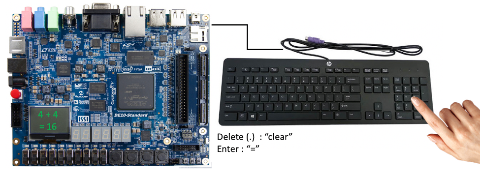
Fig. 1: General interaction of the project components.
Design Description
Figures 2 shows at a signal level how the modules for the PS2 keyboard are interconnected so that the ALU can calculate the operation with help of a decoder which detects the key being pressed, then passes through a comparator which is going to tell if either an operator or the enter key was pressed in order to save operand A and B to the ALU so the answer can be calculated. A register is also implemented for the opcode which also comes from the key detection and the +/− signal so that the ALU knows which operation is going to make.
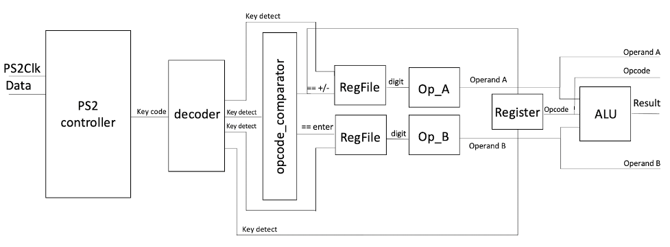
Fig. 2: Design at signal level.
Reg Slave Interface
Figure 3 shows the layout of this communication interface called reg slave interface which is made of 5 registers which have their own write port, reset and clock. For the slave interface we have a read data port and a read address port. As seen in the figure, each register had an input that came from the output of the module of the ALU working with the PS2 keyboard, and as each name suggests the four registers were storing the operands, the operator, the result and status, which pass through a demuxer in which the read address that comes from the slave selects it and sends it to the read data back to the slave.
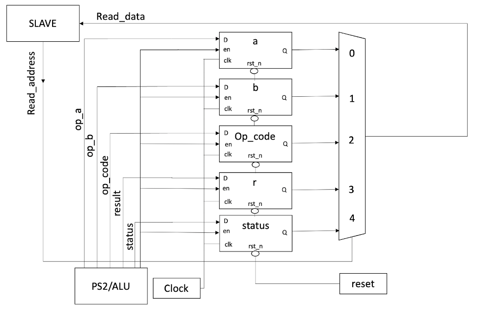
Fig. 3: Reg slave interface design.
System Qsys Design
In order to start the communication with the FPGA, some previous steps on Quartus Prime needed to be implemented. The Intel Qsys tool allows a digital system to be designed by interconnecting selected Qsys components, such as processors, memory controllers, parallel and serial ports, and the like. The Qsys tool includes many predesigned components that may be selected for inclusion in a designed system, and it is also possible for users to create their own custom Qsys components. Each component in the system, referred to as a Qsys component, adheres to at least one of the Avalon Interfaces supported by Qsys. With the interface defined for the component, Qsys is able to construct an interconnect structure, called the Avalon Interconnect, which enables components to exchange data. In this case a system for the calculator was generated based on the selected set of components and user parameters. The generated system contains Verilog code for each component and the interconnect structure, allowing it to be synthesized, placed and routed for an FPGA device. After creating the Qsys component with its respective interfaces and signals, it is now ready to make the connections to attach the register component to the required clock and reset signals, as well as to the data master port of the Nios II processor. It was noticeable in figures 4 and 5 that in the Base address column the assigned address of the new register component is 0x0000 0100. This address was assigned automatically by using the Assign Base Addresses command in the System menu. The HDL is now generated and we could now move on to the C coding for Linux application.
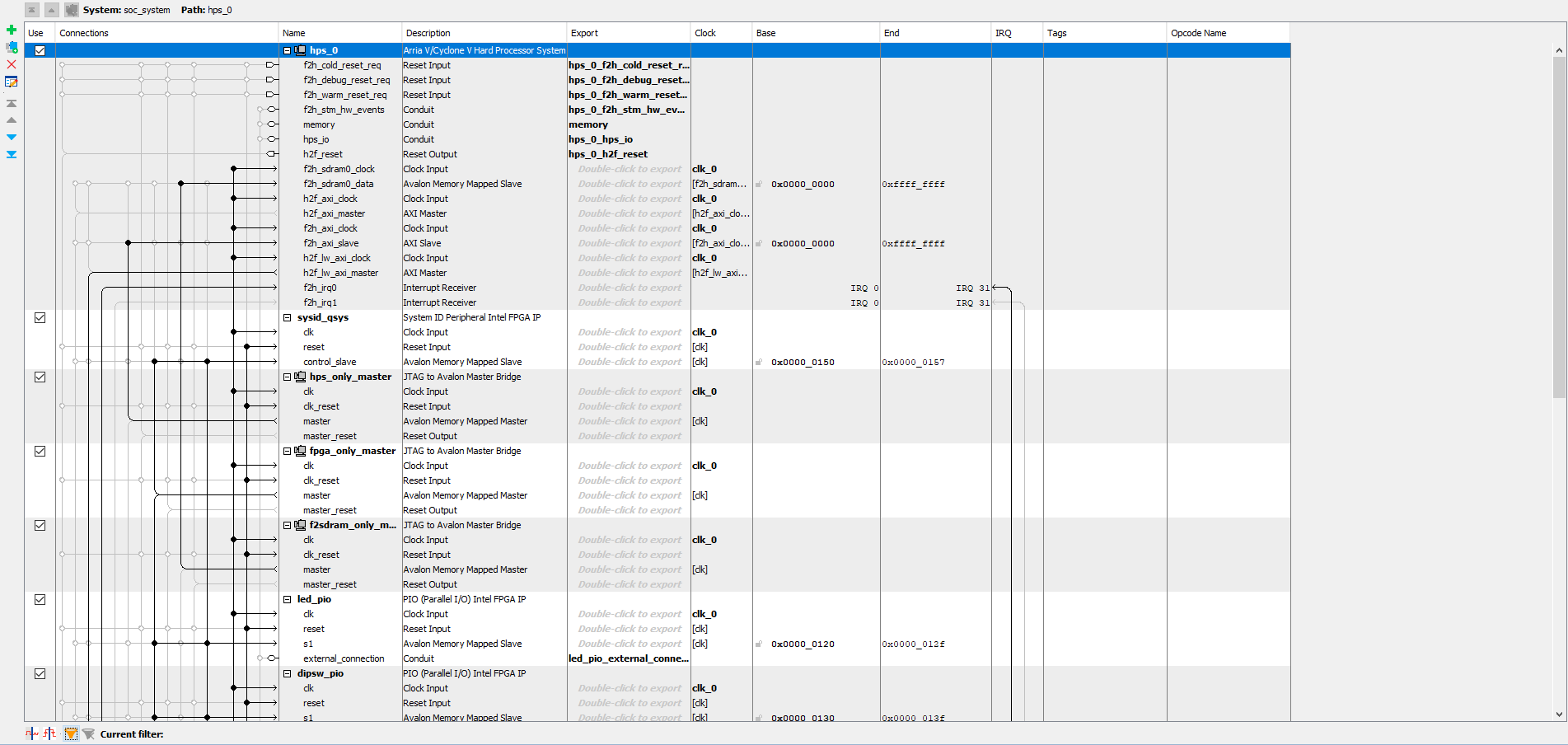
Fig. 4: System design in Qsys.
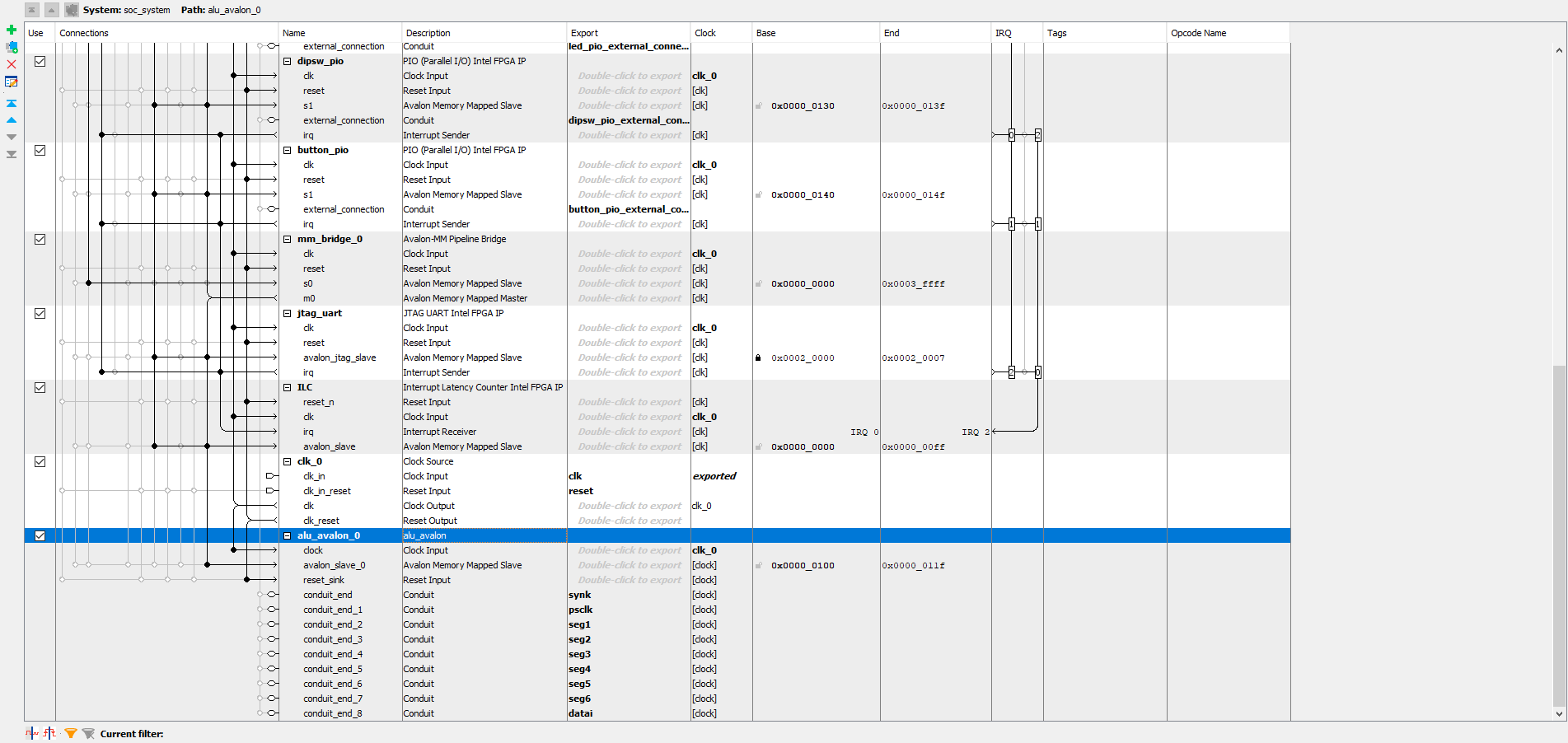
Fig. 5: System design in Qsys.
Figure 6 shows the component made with the Qsys tool. In order to make this component, the DE10_Standard_GHRD.v file was used to create the connections to the important inputs constructed as interfaces such as the avalon slave, the address, read data, the reset and the PS2 clock, for the signals that went into the seven segments, some conduits interfaces were made to wire them as shown in the figure.
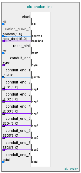
Fig. 6: Alu avalon block symbol.
Test Results
The testbench made for the simulation included the system’s and the PS2 clock, the reset and the data from the PS2. First a test for a single pressing is made by sending 8’h30 the 8’hF0 and 8’h30 again, and for the stability test was sent a double data of 8’h31 then 8’hF0 and 8’h31 again to simulate a key being pressed for a short amount of time and then released. The final simulation of the PS2 Keyboard is shown in figures 7, 8 and 9. These figures show that the test passed through the variable of SCANCODE showing those entered values.
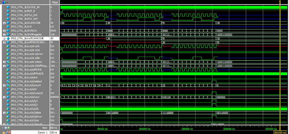
Fig. 7: PS2 Keyboard Testbench Part 1.
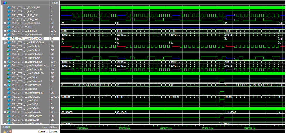
Fig. 8: PS2 Keyboard Testbench Part 2.
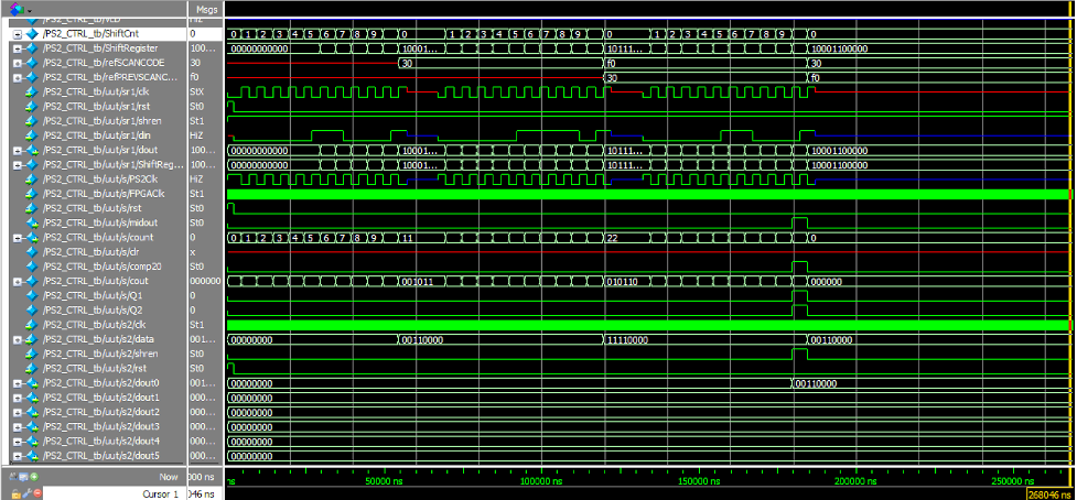
Fig. 9: PS2 Keyboard Testbench Part 3.
Video
Project demostration Youtube video